

The wafer-scale 2D semiconductor platform powering the next generation of AI chips
We enable foundries to scale advanced nodes beyond silicon for ultra-low-power compute.
BACKED BY



Beyond silicon
Next-generation AI infrastructure demands unprecedented transistor density without compromising energy efficiency.
As silicon approaches its scaling limit, foundries face a critical bottleneck:
The industry lacks the production tools to grow 2D materials on standard 12-inch wafers at commercially viable yields.

North Star™
Purpose-built for
wafer-scale 2D TMD
growth.


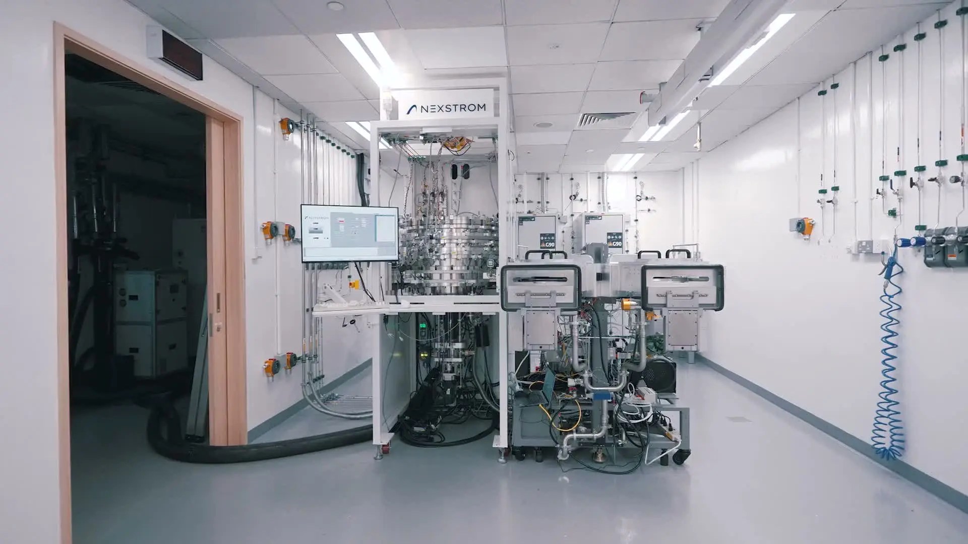
Our full-stack platform replaces legacy silicon channels with TMDs at the core of each transistor – atomically thin crystals that flawlessly conduct electricity at the sub-nanometer scale.
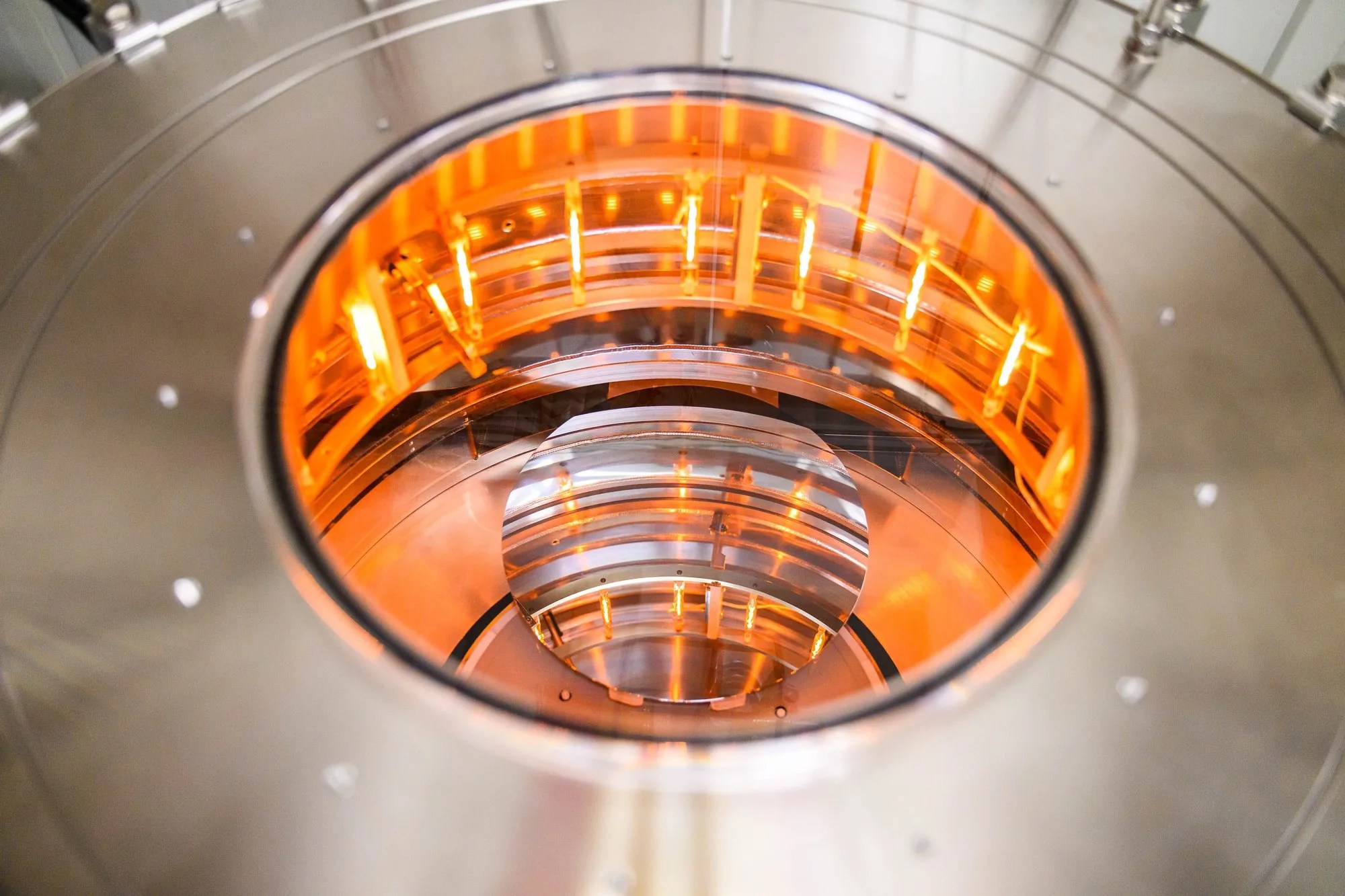
Engineered Precursor Delivery
Precise vapor-phase delivery for stable chemistry and repeatable process windows.
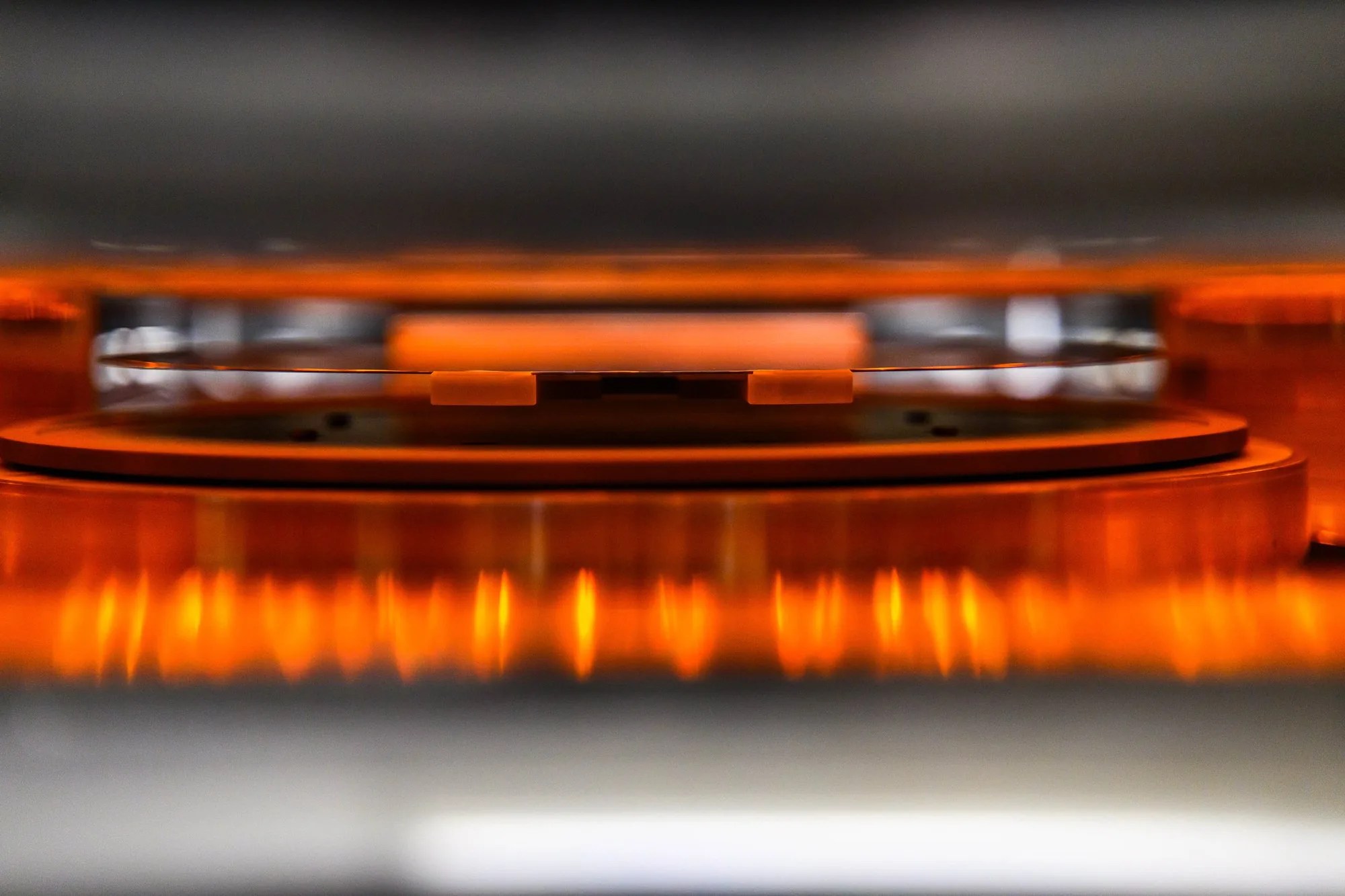
Intermediate-Reaction Showerhead
Multi-channel thermal control enables uniform precursor reactions and wafer-scale distribution.
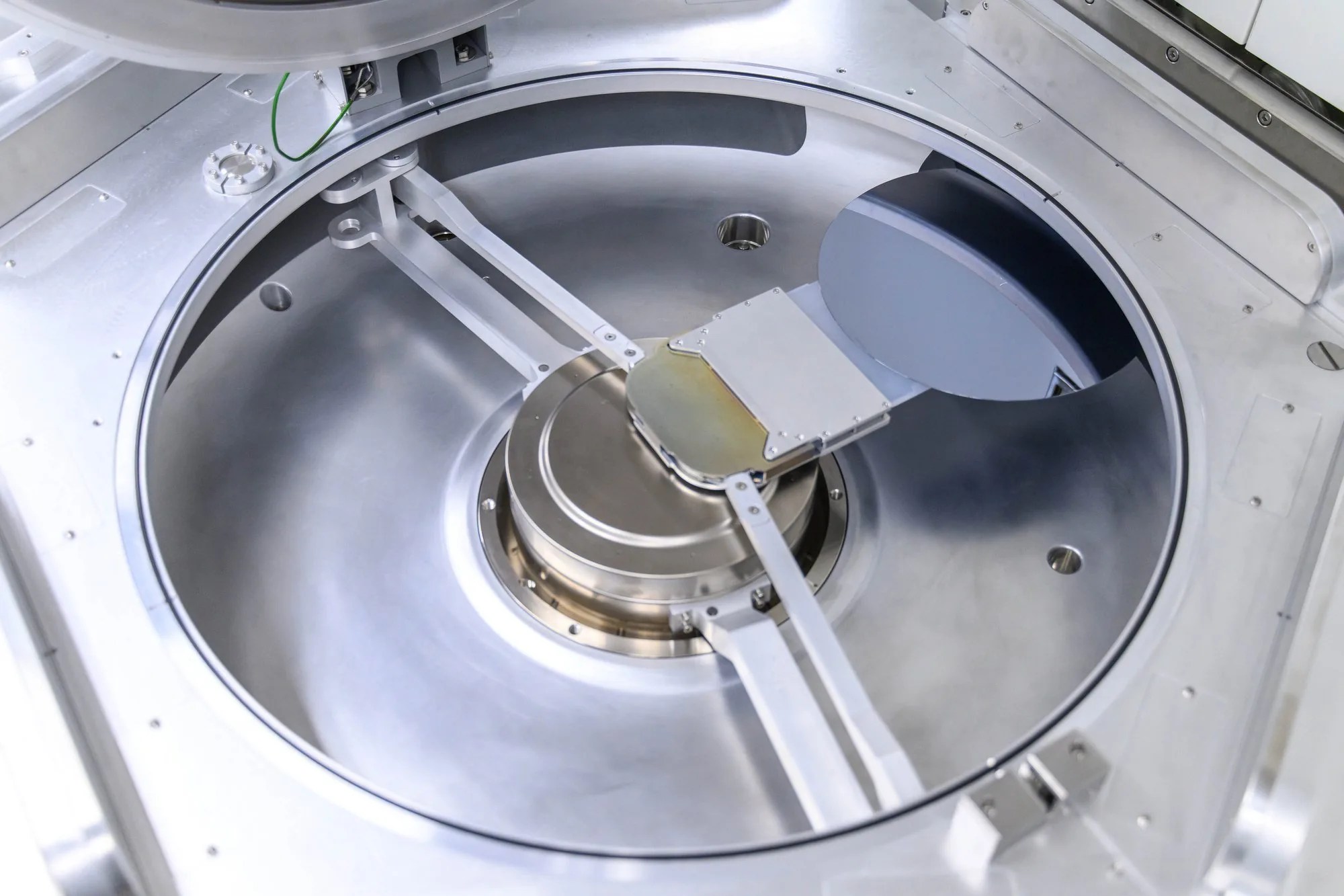
Foundry-Compatible Wafer Handling
Automated wafer transfer designed to integrate with industry-standard fab workflows.
North Star™
Purpose-built for wafer-scale 2D TMD growth.
Our full-stack platform replaces legacy silicon channels with TMDs at the core of each transistor – atomically thin crystals that flawlessly conduct electricity at the sub-nanometer scale.
Engineered Precursor Delivery
Precise vapor-phase delivery for stable chemistry and repeatable process windows.
Intermediate-Reaction Showerhead
Multi-channel thermal control enables uniform precursor reactions and wafer-scale distribution.
Foundry-Compatible Wafer Handling
Automated wafer transfer designed to integrate with industry-standard fab workflows.


Transistors built for the Angstrom era.
Up to
100×
Lower Defect Density
Eliminates micro-voids and interface flaws at atomic scales, unlocking the high manufacturing yields required for 300mm wafers.
Up to
75%
Less Switching Power
Delivers perfect gate control and low-leakage current, allowing AI chips to complete more compute operations with the same energy budget.
Over
2×
Smaller Gate Length
Reduces transistor channel length from using atomically thin 2D materials, enabling continued scaling beyond the sub-1 nm node.
AS FEATURED ON






To change what’s possible, we have to question the limits we’ve accepted.
This belief continually drives Dr. Lance Li, Co-founder & Chief Scientist of Nexstrom, and one of the earliest pioneers of 2D material growth.
From being among the first to grow single-crystal MoS₂ since 2012, to leading corporate research at TSMC, Lance has spent his career pushing the boundaries of post-silicon electronics.
His deep expertise in materials science and atomic-layer chemistry, coupled with the team’s experiences in hardware design and semiconductor integration, anchors Nexstrom’s mission: To develop wafer-scale, CMOS-compatible 2D platforms for the next generation of computing.
For Nexstrom, the Angstrom Era isn’t a theory. It’s underway — and we are building the foundation to lead it.

Timeline
We’re moving fast.
Investment
Platform foundation
- Founded by Lance Li and Xora Innovation
- Validated proprietary wafer-scale TMD growth platform for high-quality 2D semiconductors
- Established the core intellectual property and technology roadmap
Build
Lab to fab scaling
- Advanced MOCVD platform from pilot to 100mm wafer scale
- Expanded IP portfolio to cover TMD epitaxial growth, transfer processes, and device integration
- Demonstrated reproducible wafer-scale growth with high uniformity and process stability
Scale
Commercial traction
- Achieved commercial-grade TMD synthesis on 300mm wafers
- Delivered wafer samples to industry partners within 18 months of launch
- Raised US$15M in capital, including US$12M Seed round and US$3M non-dilutive funds
- Established 7 active patent families including an issued US foundational patent
- Expanded strategic collaborations with leading semiconductor manufacturers and research institutions
Team, Board & Advisors
Built with Semiconductor Industry Depth
Leadership
-

Dr. Lance Li
Co-Founder & Chief Scientist
Distinguished Professor, NUS
Former Director, TSMC -

Dr. Phoebe Tan
Co-Founder & CEO
Partner, Xora
-

Chin Kah Fai
Chief of Staff
Co-founder, Structo
-

Dr. Sung-Yen Wei
Director of Engineering
Former CEO, SulfurScience Technology
-

Dr. Jing-Kai Huang
Head of R&D
Former Asst Professor, CityU Hong Kong
-

Dr. Ang-Yu Lu
Head of System
Former Principal Engineer, TSMC
Board & Advisors
-

Phil Inagaki
Board Director
Managing Partner & CIO, Xora
-

Dr. Sundar Ramamurthy
Independent Director
Corporate Advisor, Temasek
Former General Manager, Applied Materials -

Dr. Philip Wong
Advisor
Inez Kerr Bell Professor, Stanford University
-

Dr. Aaron Thean
Advisor
Deputy President (Academic Affairs) & Provost, NUS
Former VP of Logic Technologies, imec -
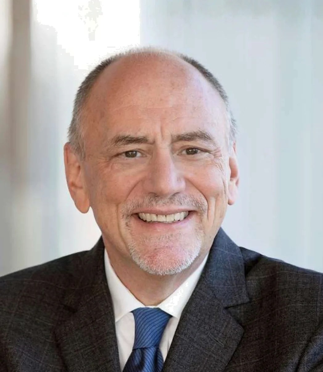
Dr. John Langan
Advisor
Former EVP/CTO, EMD Electronics
WE’RE HIRING
Build what comes next with us.
We are growing our team in Singapore across engineering, science and operations. Join us in building a post-silicon future.
Technical Resources